Blog

What Is an FPGA Chip and How Does It Work?

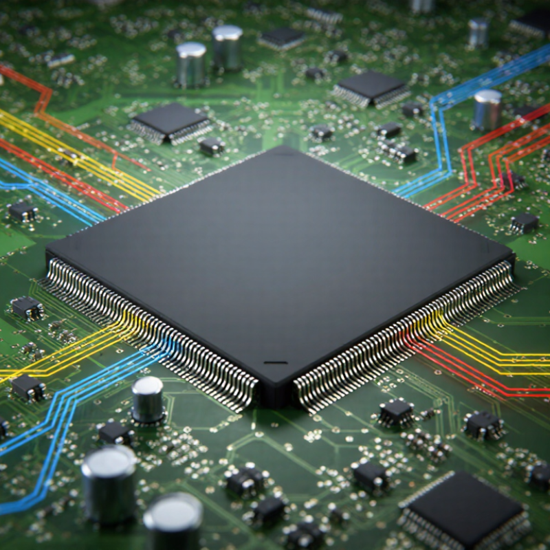
An Fpga Chip is a programmable semiconductor that lets engineers configure digital hardware after manufacturing. Unlike a fixed-function processor, it contains configurable logic blocks, routing channels, memory, and input/output resources. These elements are connected through a hardware description language, such as Verilog or VHDL. The result is a circuit designed for a specific task.

That flexibility explains its role in modern systems. MarketsandMarkets’ 2024 FPGA Market report describes growing demand from telecommunications, automotive electronics, aerospace, and artificial intelligence infrastructure. The report links this growth to faster data processing and shorter product-development cycles. Fortune Business Insights also identifies expanding FPGA adoption in edge computing and industrial automation. These findings are useful, but market forecasts remain estimates, not guarantees.

At the board level, an Fpga Chip may receive sensor data, process it in parallel, and deliver an output within microseconds. A logic block can perform arithmetic while another manages communication. This parallel structure often reduces latency compared with sequential software execution. It can also increase design complexity, power consumption, and verification effort. Faster is not always better.

Understanding the chip requires more than memorizing its architecture. Engineers must examine timing constraints, signal integrity, thermal limits, and firmware interaction. Reports from the Semiconductor Industry Association emphasize the strategic importance of resilient semiconductor supply chains. However, industry statistics rarely capture the debugging hours behind a reliable design. That practical gap matters. This guide explains how FPGA architecture, configuration, and real-world operation connect.
What Is an FPGA Chip and How Does It Work?

FPGA Basics: Definition, Purpose, and Core Characteristics

What Is an FPGA Chip and How Does It Work?

An FPGA, or field-programmable gate array, is a digital chip that users can configure after manufacturing. Unlike a fixed processor, it does not follow one permanent hardware path. Its internal fabric contains logic blocks, flip-flops, memory elements, and programmable routing channels. Engineers connect these resources to create circuits for specific tasks.

The purpose of an FPGA is flexible hardware acceleration. It can process several operations in parallel, often with predictable timing. A camera system might use it to filter pixels as they arrive. A control device could respond to sensor changes within carefully measured delays. Engineers usually describe the circuit with a hardware language, simulate its behavior, and then load the configuration into the chip. Timing still matters.

Core characteristics include reconfigurability, parallel execution, and direct control over data movement. Many devices also provide high-speed input connections, embedded memory, and arithmetic blocks. In practical development, I would inspect signal timing with test equipment and compare results against simulation. Small design errors can produce unstable outputs. That part is easy to underestimate. A circuit may work during a short test, then fail when temperature, clock speed, or input activity changes. Reliable FPGA work therefore depends on clear requirements, repeatable tests, and careful review of power and timing limits. A faster circuit is not always a better circuit.

FPGA Architecture: Logic Blocks, Routing, and Programmable Connections

An FPGA chip is a configurable digital circuit built from small logic blocks, flexible routing, and programmable connections. Unlike a fixed processor, it can be reshaped for a specific task after manufacturing. This makes its internal structure unusually important.

A logic block usually contains a lookup table, storage elements, and control circuitry. The lookup table receives input signals and produces a chosen output pattern. Flip-flops can hold results between clock cycles. Think of each block as a small workbench. It performs simple operations, then passes data onward.

Routing resources connect these blocks across the chip. Programmable switches decide which signals travel between nearby or distant areas. During configuration, a bitstream sets those switches and defines the circuit’s behavior. A practical design might send sensor data into one block, store it in registers, and route it toward a communication interface. The path is not always short. Long routes can increase delay and power use.

Timing needs careful measurement. A design may work in simulation yet fail at a real clock speed. That gap is easy to underestimate. Engineers inspect routing reports, check setup and hold requirements, and test signals on physical hardware. The architecture looks orderly in diagrams, but congestion can make it less predictable. That is where experience matters. A cleaner arrangement often beats a clever but crowded one.

How FPGA Chips Process Data Through Configurable Hardware

What Is an FPGA Chip and How Does It Work?

An FPGA chip is a programmable device built from configurable hardware blocks. Unlike a fixed processor, it can reshape its internal logic for a specific task. Engineers describe this structure with hardware description languages. The design becomes a configuration file, often called a bitstream. That file controls logic cells, memory blocks, signal routes, and input-output connections.

How FPGA Chips Process Data Through Configurable Hardware

Data does not need to wait for one central instruction stream. Several operations can run at the same time. For example, one logic section may filter sensor readings while another calculates an average. Flip-flops store clocked values, while lookup tables perform Boolean operations. Dedicated memory blocks hold temporary data close to the processing path. This short physical distance can reduce delay.

A practical test might send eight-bit samples through a moving-average filter. The FPGA receives each sample, stores recent values, adds them in parallel, and outputs the result on a predictable clock cycle. Timing tools then check whether every signal arrives before the next clock edge. Small routing changes can affect that result. That detail is easy to underestimate.

FPGAs offer speed and flexibility, but they are not automatically efficient. Poorly planned data paths can waste logic and power. Debugging may also feel less direct than testing software. A waveform can reveal the failure, yet the cause may sit several hardware layers away. Careful simulation, timing analysis, and repeated testing remain essential.

What Is an FPGA Chip and How Does It Work?

This waveform illustrates an 8-cycle FPGA datapath. A configurable lookup table implements the Boolean function Y = (A AND B) XOR C, allowing the output to be produced directly by programmable hardware.

How to read it: A, B, and C are input signals sampled on each clock cycle. The Y signal is the resulting hardware output. Unlike software that executes instructions sequentially, FPGA logic can process these signal paths in parallel during each clock period.

FPGA Programming: From Hardware Description to Configuration

An FPGA is a reconfigurable chip built from logic blocks, routing channels, and memory resources. Its behavior begins in hardware description language, not ordinary software code. Engineers describe registers, counters, data paths, and timing relationships. Synthesis converts that description into a logic network. Place-and-route then maps the network onto physical chip resources.

The final output is a configuration bitstream. After power-up, the device loads this bitstream into configuration memory, creating the intended circuit. A clock edge can trigger a register, while nearby routing carries its result to the next operation. This process demands timing analysis, simulation, and hardware testing. A 2024 global FPGA market report estimated the sector at approximately 9.7 billion US dollars in 2023, with continued growth through 2030. That expansion reflects demand for adaptable acceleration and real-time processing, but market size does not guarantee a reliable design.

Practical experience suggests starting with a small module and checking waveforms before adding complex pipelines. Tips: define clock domains clearly, constrain timing early, and inspect resource utilization after every major change. Keep reset logic simple. A design may simulate correctly yet fail on hardware because of timing uncertainty, electrical noise, or an overlooked constraint. I still find this step easy to underestimate. The bitstream is not merely compiled code; it is a physical arrangement that must behave predictably under real temperature, voltage, and workload conditions.

What Is an FPGA Chip and How Does It Work? — FPGA Programming: From Hardware Description to Configuration
Data Dimension Typical FPGA Characteristic How It Works Programming or Design Relevance
Core Definition Reconfigurable digital integrated circuit An FPGA contains programmable logic resources and configurable interconnections that can be arranged to implement different digital circuits. The same device can support multiple hardware designs without changing the physical chip.
Primary Logic Element Look-up table and flip-flop A look-up table implements combinational logic, while a flip-flop stores a value and supports synchronous sequential logic. Designers combine these elements to create counters, state machines, arithmetic units, control logic, and data-processing pipelines.
Look-Up Table Function Truth-table-based logic implementation The LUT uses configuration memory to select an output for each possible input combination. A common modern LUT structure supports several input variables. LUT size affects how efficiently Boolean functions and portions of larger logic expressions can be implemented.
Configurable Interconnect Programmable routing network Switch matrices and routing channels connect logic elements, memory blocks, input/output resources, and specialized processing blocks. Routing quality influences timing, power consumption, resource utilization, and the maximum operating frequency.
Configuration Storage Volatile or non-volatile configuration memory Many FPGAs load configuration data from external storage after power-up, while some devices retain configuration internally. A design may need a boot-time configuration process before the FPGA begins normal operation.
Hardware Description Register-transfer-level design description Hardware description languages express registers, combinational operations, clock relationships, interfaces, and data movement. The description defines hardware behavior and structure rather than a sequence of instructions executed by a conventional processor.
Synthesis HDL or high-level design converted into logic Synthesis analyzes the design, performs logic optimization, and maps supported operations to LUTs, flip-flops, memories, and specialized blocks. Coding style, inferred hardware, constraints, and arithmetic choices can significantly affect area and performance.
Implementation Placement and routing The implementation process assigns logical elements to physical locations and creates routes between them while attempting to satisfy design constraints. A design is not ready for hardware use until timing, connectivity, and resource checks are completed successfully.
Configuration File Binary programming data The completed implementation is converted into a device-specific configuration file containing settings for logic, routing, memory initialization, and I/O behavior. The file is transferred to the FPGA through a supported programming interface or loaded automatically during system startup.
Embedded Memory Block RAM and distributed memory Dedicated memory blocks provide efficient storage for buffers, tables, queues, instruction storage, and intermediate data. Using dedicated memory generally preserves LUT resources and supports synchronous read/write designs.
Arithmetic Resources Dedicated multiply-accumulate and arithmetic blocks Specialized blocks accelerate multiplication, addition, accumulation, filtering, and other common numeric operations. Mapping arithmetic to dedicated resources can improve throughput and reduce general-purpose logic usage.
Clock Management Clock distribution and frequency-control circuitry Dedicated clock networks distribute low-skew clock signals, while clock-management circuits can adjust frequency and phase within device limits. Correct clock-domain design is essential for reliable data transfer and timing closure.
Input and Output Configurable I/O cells I/O cells connect internal logic to external signals and can support different electrical standards, directions, drive strengths, and timing features. Pin assignments and electrical constraints must match the circuit board and connected peripherals.
Parallel Processing Many operations executed concurrently Independent hardware functions operate at the same time, allowing multiple data items or pipeline stages to be processed in parallel. Parallelism can increase throughput, especially for streaming, signal-processing, image-processing, and control applications.
Pipelining Computation divided across clocked stages Registers separate processing stages so different data items can occupy different stages simultaneously. Pipelining often raises throughput and operating frequency, although it can add latency and consume additional registers.
Timing Constraints Clock, input, output, and path requirements Constraints describe required clock periods, signal arrival times, output deadlines, and relationships between clock domains. Timing analysis verifies whether signals can travel through the implemented design within the required time limits.
Resource Utilization Logic, memory, arithmetic, I/O, and clock usage The design consumes a finite quantity of each physical resource available in the FPGA. Utilization reports help identify congestion, inefficient structures, and remaining capacity for future features.
Reconfiguration Hardware behavior can be changed after manufacturing A new configuration file can replace the current hardware arrangement, subject to device and system requirements. This supports field updates, application-specific hardware modes, rapid prototyping, and evolving product requirements.
Verification Simulation, assertions, and on-device testing Design behavior can be examined before programming the device, then validated with real signals and internal monitoring after configuration. Verification helps detect functional errors, clock-domain problems, reset issues, and interface timing violations.
Main Design Trade-Off Flexibility versus area, power, and performance Programmability provides adaptability, but configurable routing and general-purpose resources may require more area or power than a fixed-function circuit. Architecture, parallelism, clock frequency, data width, and memory usage must be balanced for the target application.

Common FPGA Applications, Benefits, and Limitations

An FPGA is a programmable chip built from configurable logic blocks, routing channels, and memory resources. Engineers define its hardware behavior after manufacturing. Unlike a fixed processor, it can perform many operations in parallel. A camera system, for example, may process several pixel streams inside the chip. Latency matters. The device responds in predictable clock cycles.

Applications continue expanding across industrial control, medical imaging, telecommunications, automotive sensing, and data-center acceleration. MarketsandMarkets estimated the global FPGA market at about 9.8 billion US dollars in 2024, with growth toward 13.1 billion dollars by 2029. Allied Market Research also projected strong long-term expansion, linking demand to edge computing and real-time processing. These figures suggest durable adoption, but forecasts are not guarantees.

FPGAs offer flexible updates, parallel performance, and efficient control over specialized workloads. They can reduce response delays when software processing becomes too slow. Their limitations are equally practical.

Hardware design requires specialized skills, verification time, and careful power planning. Development tools can feel unforgiving. A small timing error may disrupt an otherwise correct design. Production costs can also rise for low-volume projects. I have found that flexibility sometimes creates unnecessary complexity. The best choice depends on workload stability, latency targets, energy limits, and available engineering experience.

FrenchBulgaria